Photonics & Optical Infrastructure Insights
From PIC Design to Packaged Product: The Hidden Challenges of Silicon Photonics Commercialisation
Photonics Frontier Advisory · Published 18 October 2026 · Technical perspective
Why foundry selection, optical coupling, packaging interfaces and test strategy belong in the product plan before tape-out.
Tape-out is an interface commitment
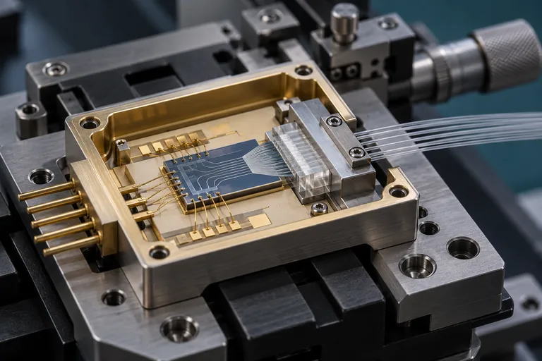
A design-rule-clean layout establishes important fabrication constraints, but it does not establish a usable module. The packaged product must connect optical paths, electrical signals, thermal control, mechanics and software. Those interfaces should be defined while design choices remain flexible. Otherwise a successful chip can arrive with inadequate probe access, incompatible fibre geometry, difficult electrical routing or insufficient calibration support. The product plan needs to name the conditions under which the device will be judged usable.
Choose a platform against the product
Foundry and PDK selection should begin with requirements: wavelength, loss budget, active functions, electrical bandwidth, temperature range and intended volume. Then examine access terms, design rules, model coverage, fabrication schedule, test options and package compatibility. A familiar toolchain or an attractive mask price cannot settle these questions alone. The relevant comparison is the route to a validated product, including engineering effort and partner dependencies, rather than the cheapest isolated fabrication step.
Coupling is a system trade-off
Grating couplers offer surface access that can be useful for wafer probing and some assembly approaches. Their performance depends on the actual design and platform, including wavelength and polarisation. Edge-coupling approaches can support broad optical bandwidth but introduce their own facet, mode-matching and alignment requirements. Neither category is universally cheaper or better. Imec’s public work illustrates both wafer-level grating-coupler testing and developments in edge-coupling interfaces; production decisions require the relevant process data and assembly method.
Define packaging ownership early
An OSAT or specialist photonics assembler needs more than a die drawing. Agree optical and electrical interfaces, adhesives and materials constraints, thermal paths, fixtures, inspection, acceptance tests and failure-analysis responsibilities. Clarify who owns the package design and changes, who procures parts, and how a nonconforming assembly is investigated. A partner may be highly capable yet unsuited to a particular low-volume prototype or alignment method. Capability, available capacity and willingness to support the programme are distinct selection criteria.
Test before expensive value is added
Wafer probing can identify problems before assembly where the design and test method permit it. It does not replace packaged-module validation. Package stress, fibre attachment, electrical interconnects, thermal behaviour and control electronics can introduce new effects. Define how wafer measurements correlate with module performance, and which measurements are release criteria at each stage. Calibration time, test automation and fault diagnosis belong in the cost and schedule model alongside fabrication and packaging.
Commercialisation needs contractual interfaces too
Background IP, newly created IP, design files, process access, test software and ownership of fixtures should be addressed in partner scopes. Product acceptance should be measurable and distinguish supplier deliverables from system-level outcomes. Export review depends on the actual item, transaction, destination, end user and end use; a generic PIC label cannot settle it. A disciplined programme connects these technical and commercial interfaces into staged decisions, making the prototype a source of evidence for the next investment rather than the end of the plan.
Questions for your next review
- What evidence supports the conclusion, and what remains an assumption?
- Which qualification or manufacturing gate could change the commercial outcome?
- What additional records, tests or partner commitments would resolve the uncertainty?
Selected technical references
Public technical context reviewed for this article. Supplier material describes that supplier’s architecture; it is not independent proof of market adoption. The assessment framework above is original advisory analysis.
General technical analysis; no confidential employer or client information is used. No investment recommendation or guaranteed outcome is provided.
Related service: Silicon Photonics & PIC Productisation