From experiment to adoption
Why a promising photonic chip takes time to become everyday technology
Packaging, testing and maintenance explain much of the journey from an impressive demonstration to useful infrastructure.
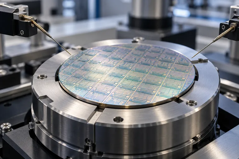
A successful chip demonstration is a beginning. Turning it into a technology that people can deploy repeatedly is a different kind of achievement. Photonics makes this distinction especially visible because light must travel through a physical chain of devices, interfaces and connections.
The package is part of the technology
A photonic die needs a way to receive and deliver light, exchange electrical signals and operate within a manageable thermal environment. Fibres, connectors, laser sources and electronic components all influence the final result. An elegant optical circuit can become difficult to use if its interfaces are fragile or expensive to assemble.
NVIDIA describes its co-packaged-optics platform as the work of an ecosystem spanning silicon photonics, electronics, lasers, fibre and packaging. That is a useful illustration of why adoption involves more than selecting a chip.
Repeatability changes the conversation
Research asks whether an idea can work. Manufacturing asks how consistently it works across devices, operating conditions and time. Test coverage, assembly yield and calibration can change the economics even when the underlying optical design performs well.
In an AI installation, replacement and diagnosis matter as well. A densely integrated product may offer performance advantages while requiring a different maintenance approach. The practical choice depends on the operator, the equipment and the intended use.
Watch the surrounding progress
When following photonics trends, look for evidence beyond an isolated performance record: repeatable packaged devices, clear test methods, compatibility with the surrounding system and a credible plan for operation and repair.
There is no single adoption timetable for all photonic technologies. Optical communication, emerging optical I/O and experimental optical computing start from different positions. What they share is an enjoyable engineering puzzle: bringing the physics, the package and the real-world task into alignment.
Further reading
An independent educational note based on public sources. Interpretations and questions here are editorial perspectives; linked product descriptions are the suppliers’ own accounts.